Members: Hans Robinson, TBD Collaborators: MicroXact, Inc (Lead organization), Sundew Technologies |
|||||
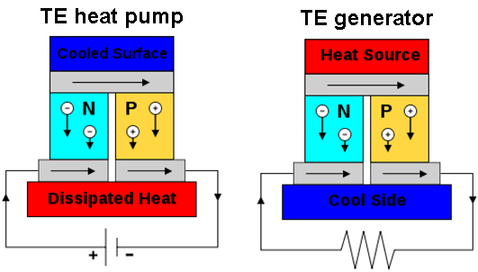
Thermoelectric (TE) materials have the property that electric current is accomanied by a flow of heat and vice versa. This naturally leads to its two main applications; as the active material in heat pumps and in power generators. Thermoelectrics can in other words replace compressors and turbines with a light-weight and compact solid state solution with no moving parts. |
 |
||||
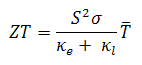
Unfortunately, the efficiency of TE devices is quite low, and they are currently only competitive in applications where space and weight is at a premium, such as portable coolers and in power generation in satellites. The improvement of TE efficiency is therefore currently a major research topic. The efficiency of a TE material is characterized by its figure of merit ZT, which is given by
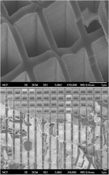
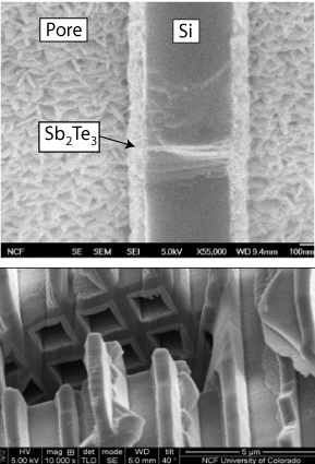
where σ is the electrical conductivity of the material, κe and κl are the electronic and lattice thermal conductivities, S is the Seebeck coefficient, and T is the average temperature of the material. Optimizing ZT is rather difficult since the parameters tend to be related in unfavorable ways. For instance, increasing σ also increases κe and decreases S. For this reason, unstructured bulk materials tend to have ZT values no larger than 1, where values well in excess of 2 are required if TE materials are to find applications outside of their current niches. ZT can be increased by engineering the TE material with two goals in mind. First, the density of states should be made as asymmetric as possible near the fermi energy, which maximizes S for a given conductivity. Second, the scattering rate for phonons should be maximized as much as possible so as to reduce the value of κl. The latter approach has proven the most successful, and is accomplished by structuring the material at the nanoscale to provide as many opportunities for phonon scattering as possible. Simply introducing disorder in the material is however not enough, since that tends to also reduce the electron mobility, cancelling the improvment provided by a lower κl. The best results of this kind have been obtained in superlattices grown with epitaxial techniques, where well-defined and ordered interfaces between similar materials can provide phonon scattering without adversely affecting electron conductivity. The drawback is that these techniques only allow materials to be fabricated in thin films of no more than about a micron in thickness, while practical TE devices require materials thicknesses on the order of hundreds of microns at least. In this project, we plan to overcome this limitation by growing nanostructured TE films onto macroporous silicon (MPSi) using atomic layer deposition (ALD), which will allow micron-thick thin films to be arranged into materials thick enough for practical devices
The MPSi provides a large, vertically oriented surface area for growth of TE materials, so that mm thick epitaxial films naturally form a structure several hundred mm thick. The Si scaffold can be made thin enough that its impact on device performance in many cases is negligible. ALD is an epitaxial growth technique where precursor compounds are sequentially brought into the chamber to react with the substrate. The precursors are chosen such that they do not react with themselves, so that two or more different precursors must be brought in to form a single monolayer on the substrate. The substrate temperature is kept high enough that physisorption of multiple layers of the precursor does not occur, but low enough that a monolayer of the precursor can form on the surface. Since only one of the precursors is present at any one time, the process is self-limiting, depositing no more than a single atomic layer per cycle. Since precursor concentration and exposure time have little influence on deposition rate in an a properly optimized process, we can expect the same film thickness at the bottom of an MPSi structure as at the top, which is ideal for this application.
This project is undertaken in collaboration with MicroXact, Inc (which is leading the project and supplies modelling and MPSi fabrication expertise) and Sundew Technologies (a world leader in ALD equipment and growth methods). Our role in this project is to characterize materials and nanostructures for structural and thermoelectrical transport properties, which will entail a fairly extensive effort, as ALD grown tellurides are novel, where very little published work extists. |
|||||